0 item(s)

CD4071B, CD4072B and CD4075B OR gates provide the system designer with direct implementation of the positive-logic OR function and supplement the existing family of CMOS gates.
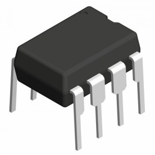
The CD4071B, CD4072B, and CD4075B types are supplied in 14-lead hermetic dual-in-line ceramic packages (F3A suffix), 14-lead dual-in-line plastic packages (E suffix), 14-lead small-outline packages (M, MT, M96, and NSR suffixes) and 14-lead thin shrink small-outline packages (PW and PWR suffixes).
| Attribute | Value |
|---|---|
| Logic Function | OR |
| Mounting Type | Through Hole |
| Number of Elements | 4 |
| Number of Inputs per Gate | 2 |
| Schmitt Trigger Input | No |
| Package Type | PDIP |
| Pin Count | 14 |
| Logic Family | 4000 |
| Maximum Operating Supply Voltage | 18 V |
| Maximum High Level Output Current | -4.2mA |
| Maximum Propagation Delay Time @ Maximum CL | 90 ns @ 15 V, 120 ns @ 10 V, 250 ns @ 5 V |
| Minimum Operating Supply Voltage | 3 V |
| Maximum Low Level Output Current | 4.2mA |
| Width | 6.35mm |
| Dimensions | 19.3 x 6.35 x 4.57mm |
| Length | 19.3mm |
| Minimum Operating Temperature | -55 °C |
| Maximum Operating Temperature | +125 °C |
| Height | 4.57mm |
| Propagation Delay Test Condition | 50pF |
Your order will be dispatched within 3-5 working days. Most deliveries require someone to accept and sign for the delivery to ensure the goods are received correctly. To help you we can arrange for delivery to be made elsewhere. Click here for more information.
We hope you like your purchase, however, if you are not entirely satisfied with any item, it can be sent back to us for a refund, provided it is returned within 14 days after delivery has been made (unless otherwise specified). Please click here for more information.


